Scalable optical systems must grow in capacity without forcing every generation to restart its component architecture. They look for platforms that can extend channel count, data rate, or modulation format while preserving familiar interfaces and qualification methods.
This reduces redesign work and gives supply, manufacturing, and operations teams time to prepare for higher volumes. Integration contributes by bringing repeatable optical functions onto a common substrate. It can reduce discrete alignments and interconnects, improve channel matching, and establish reusable building blocks.
However, integration also concentrates risk: one process shift, package limitation, or thermal issue may affect many functions simultaneously. Scalability therefore depends on control as much as density.
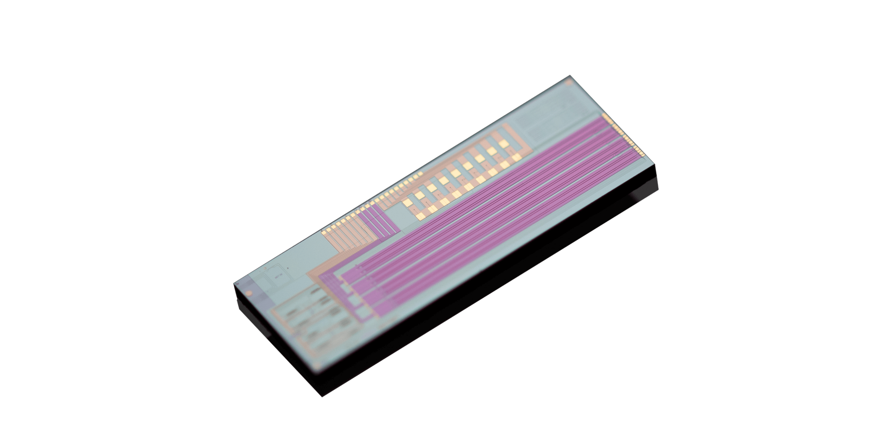
The published range of TFLN chips illustrates a platform spanning 800G, 1.6T, and 3.2T designs, alongside coherent ZR and custom intensity-modulator products. They interpret this breadth as a starting point for roadmap evaluation. The decisive evidence is whether design rules, fabrication, packaging, and test can support each step with predictable performance and supply.
Scaling Requires a Reusable Functional Platform
A reusable platform begins with stable material and process assumptions. Integrated photonic chips should share waveguide geometry, electrode concepts, coupling methods, and design verification wherever practical. Common foundations can shorten development because previously characterized loss, bandwidth, and reliability behavior remains relevant.
Exceptions must be documented so that a new product does not inherit invalid assumptions from an earlier generation. For TFLN chips, the electro-optic function is central. Thin-film lithium niobate can support intensity, IQ, and polarization-division-multiplexed modulation.
These blocks address different links, yet they can draw on related fabrication knowledge. They ask which layers, lithography steps, wafer tests, and package interfaces are genuinely common, because platform value comes from repeatable reuse rather than shared branding. Channel scaling also requires uniformity.
An eight-lane device must maintain acceptable bandwidth, voltage, extinction, and coupling across all paths. They review distributions rather than averages and model the impact of a limiting lane on module yield. This is especially important when several channels are integrated on one die and cannot be economically replaced individually.
Multiple Rates Must Share More Than a Marketing Roadmap
The roadmap moves from a 70 GHz 1.6T DR8 or 800G DR4 product to a listed 110 GHz 3.2T DR8 product. That progression suggests greater electrical and optical demands, not merely a doubled label. Integrated photonic chips must remain compatible with drivers, fibers, packaging materials, and test equipment that may evolve at different speeds.
Coherent applications add another axis. A 70 GHz PDMIQ device for 800G and 1.6T ZR uses lower listed insertion loss than the multi-lane direct-detection products, while its differential half-wave voltage is higher.
When comparing TFLN chips across formats, they avoid treating one specification as preferable in every architecture; each architecture assigns value differently to loss, voltage, complexity, and reach. A scalable commercial plan includes intermediate products and migration paths.
Customers may deploy 800G for years while developing 1.6T, and early 3.2T trials may coexist with both. They favor interfaces and qualification records that allow mixed generations to be supported, since abrupt replacement would create inventory, training, and interoperability burdens throughout the supply chain.
Operational Control Completes the Meaning of Integration
Integration extends beyond the optical circuit. Bias controllers, drivers, thermal sensors, firmware, calibration data, and diagnostic interfaces determine how the device behaves in operation. For integrated photonic chips, they define ownership of each control loop and specify how a module reports drift or degradation.
Otherwise, dense functionality can become difficult to observe and maintain. Production monitoring for TFLN chips should capture wafer lot, die location, coupling data, RF response, voltage, and extinction characteristics. Linking those records to final module results helps locate yield loss and supports corrective action.
They also request notification thresholds for material, mask, process, or package changes that could shift a previously qualified performance distribution. Service strategy deserves equal attention. Highly integrated modules may be replaced rather than repaired, so failure analysis must recover enough evidence from returned units to protect the broader fleet.
They plan spare levels, diagnostic procedures, and supplier escalation paths before deployment. This keeps scale from turning small unexplained variations into widespread operational uncertainty. Scalability also changes validation economics.
Reusing fixtures, software, reference modules, and trained personnel can reduce the cost of each new rate. They track which assets remain valid and which need higher-bandwidth replacement, allowing capital planning to follow the technical roadmap instead of reacting after prototypes arrive.
They assess scalability through a chain of evidence: reusable design rules, measured lane uniformity, compatible packaging, production test capacity, and controlled lifecycle changes.
Data-rate announcements are relevant, but they do not substitute for this foundation. A platform earns confidence when each new product can build on verified knowledge without hiding new dependencies.
The purchasing decision should therefore include roadmap governance. Engineering, operations, and commercial teams need scheduled reviews of qualification progress, capacity commitments, cost trends, and field feedback.
That process allows capacity growth to follow demonstrated readiness rather than a timetable driven by market headlines. Scaling an optical system depends on package yield and test throughput as much as channel count. A shared-platform study that includes Liobate devices can reveal whether added functions remain controllable across lots and production volumes.
